
Show summary Hide summary
- The Invisible Blueprint: Why This Material’s Structure Was Uncrackable—Until Now
- What MIT Saw That No One Else Did—and the Daring Methods Behind Their Discovery
- A Structure That Shouldn’t Exist? The Paradox at the Heart of the Findings
- How This Hidden Architecture Could Transform Phones, Computers, and…?
- The Unanswered Questions: What MIT’s Breakthrough Still Can’t Explain
- What Happens If the Next Secret Surfaces? The Consequences No One Saw Coming
- FAQ
- How will understanding the hidden high tech material structure impact everyday technology?
- Why was the structure of this high-tech material so difficult to analyse?
- What methods did MIT scientists use to finally reveal the high tech material structure?
- Could this discovery influence material design in other industries?
For years, industry insiders and scientists puzzled over a high-tech material that defied every attempt to uncover its true nature. Now, MIT scientists finally reveal the hidden structure of a mysterious high tech material structure—solving an enigma that resisted some of the sharpest minds in modern materials science. What they discovered is not just a technical detail. It is a roadmap to a future where the phones in our pockets, the computers on our desks, and technologies we have yet to invent may be redefined from the inside out.
This isn’t just a story of academic curiosity satisfied. The material’s elusive inner framework, visualized for the first time by MIT’s team, hints at a design so counterintuitive it could unlock faster, smaller, and more resilient devices across countless industries. The secrets exposed aren’t just clever—they are catalytic. And they raise new questions about what this breakthrough means for the tech we use every day, and for the competitive race to harness what was once invisible to all.
The Invisible Blueprint: Why This Material’s Structure Was Uncrackable—Until Now
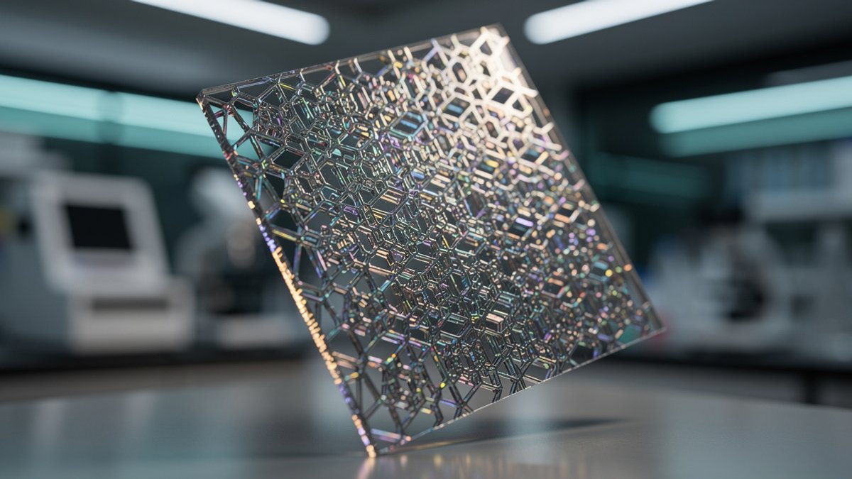
The material in question did not just puzzle researchers—it sparked frustration and admiration across top laboratories on four continents. Its properties hinted at game-changing potential, yet its atomic structure repeatedly slipped away from imaging tools that have mapped substances as complex as viruses and nanomachines. For years, the world’s finest material science experts watched as their analysis hit a wall. Even MIT researchers, known for going where others cannot, saw their initial efforts dissolve into dead ends and paradoxes.
The Story of the First Human Tool Isn’t What You Think—How One Overlooked Container Quietly Changed Everything
Deep-diving fur seals delay their heart surges—why the real recovery starts only after landfall
- What set this high-tech enigma apart was its ability to mask edges, blur patterns, and seem invisible to conventional techniques.
- Electron microscopes, which can catch single atoms in their lattice, offered only murky profiles—each snapshot missing crucial links in the hidden structure.
- X-ray diffraction, the gold standard for crystalline materials, returned data riddled with contradictions.
Every glance inside created as many new questions as it answered, reinforcing the myth: this material was uncrackable.
This scientific deadlock carried serious implications. If no one could see how the atoms were arranged, there could be no recipe to scale or harness its unique functions. Advanced imaging strategies seemed to stall at the doorstep of insight. Yet, resisting standard analysis only made the material more tantalizing—a riddle MIT researchers refused to leave unsolved, no matter how unattainable the blueprint appeared. The stage was set for a breakthrough that would ripple far beyond the lab. For broader context on transforming city infrastructure with advanced materials, consider LA’s plans for a high tech, computer-controlled subway line.
What MIT Saw That No One Else Did—and the Daring Methods Behind Their Discovery

MIT scientists realized traditional crystallography was powerless against this material’s freakish complexity. Rather than concede, the team merged cutting-edge electron microscopy with unconventional computational modeling, letting them visualize atomic patterns hidden from even the sharpest X-ray beams. Their strategy didn’t just add a new lens—it rewrote the rules of the entire discovery process.
- Early attempts were riddled with false leads.
- At one point, the team believed their models pointed in circles, hinting the material might lack any regular structure at all.
- The turning point came with an audacious experiment: ultra-precise electron bursts revealed a repeating motif, a fingerprint missed by decades of prior work.
In a moment, theory gave way to clarity. The scientific breakthrough wasn’t just technical—it shattered the illusion that this material would remain forever unknowable, positioning MIT at the frontier of high-tech innovation.
A Structure That Shouldn’t Exist? The Paradox at the Heart of the Findings
When MIT scientists finally reveal the hidden structure of a mysterious high-tech material, the reaction from the scientific community is disbelief—because the structure they found simply shouldn’t exist according to standard theoretical models. Experts were convinced that the material’s properties required a more conventional atomic arrangement, leading to years of failed attempts and dismissed theories. Yet the new evidence demonstrates a pattern that contradicts decades of foundational chemistry and physics. For a dramatic example of how unexpected discoveries can reshape knowledge, see what happened when an ancient crocodile relative challenged evolution.
This unexpected result isn’t a minor anomaly. It creates a true scientific paradox: if the structure is real, then our understanding of the forces binding advanced materials needs a serious update. Such a finding doesn’t just rewrite a line in a textbook, it forces researchers to reexamine the basic principles that guide material design. This paradox, rather than closing the case, has thrown open the door to entirely unforeseen possibilities for future technologies.
How This Hidden Architecture Could Transform Phones, Computers, and…?
- The unveiled structure could spark a wave of technology innovation with ripple effects across consumer electronics.
- By finally understanding how the atoms truly arrange themselves, device designers can exploit properties that were previously locked away. Imagine batteries with higher capacities or far faster charging, not in theory but in the palm of your hand — a direct shot into mainstream smartphones and laptops.
- For sensors, this precise microscopic layout could trigger radical boosts in sensitivity, pushing fields like medical diagnostics or environmental monitoring forward overnight.
- Applied materials companies are already eyeing the opportunity to produce components that perform leaps beyond today’s standards. The impact is not limited to performance alone.
- Lower power consumption and heat loss are now realistic, potentially rewriting the rules for everything from wearable tech to quantum computing.
To understand how breakthroughs in material science can cause paradigm shifts, explore the race to find dark matter with a student-built cosmic radio.
But the most startling prospect is still emerging. If this exotic structure can be tweaked, entirely new classes of chips or memory systems might be built — gadgets and systems we haven’t even imagined. The doors MIT has opened may soon turn marketing boasts into everyday reality.
The Unanswered Questions: What MIT’s Breakthrough Still Can’t Explain
Despite MIT’s bold reveal, the material’s newfound structure raises as many questions as it answers. Some scientists are unsettled by unexplained shifts in material behavior under pressure, which existing theories cannot account for. Open questions now dominate the scientific debate: Why does this architecture remain stable when models predict collapse? How do electrons move through its puzzling lattice, and what unknown properties might emerge at the nanoscale? For further reading on what it means to find hidden structures, see how AI models can reveal the structures of crystalline materials.
Future research is sprinting to map these anomalies, but for now, nobody can say when or if the material may upend today’s most reliable technologies. Each layer unwrapped exposes deeper mysteries—fuel for the next wave of disruptive breakthroughs, or possibly, new technological hazards.
What Happens If the Next Secret Surfaces? The Consequences No One Saw Coming
MIT’s revelation does more than solve a scientific puzzle. It throws open the doors to a new phase in the innovation pipeline, inviting both opportunity and upheaval. Now that this once-invisible structure is mapped, entire sectors are bracing for technology disruption. Overnight, established design rules for electronics or energy storage could become obsolete. Labs and corporations are chasing fresh blueprints, eyeing the chance to leap ahead—or risk getting blindsided by competitors who rethink what’s possible.
The real tension lies in the future implications that ripple outward. If one hidden structure can upend what we thought we knew, what happens when the next cryptic material yields its secrets? Expect unexpected consequences: novel devices nobody predicted, new security challenges, and perhaps even shifts in global supply chains. Researchers everywhere have been put on alert, not just to replicate MIT’s result, but to anticipate what other mysteries, now emboldened by this breakthrough, are waiting just beneath the surface. With the rules being rewritten, the real impact is just beginning.
FAQ
How will understanding the hidden high tech material structure impact everyday technology?
Uncovering the high tech material structure opens the door to creating devices that are faster, more resilient, and possibly smaller than current technology. This breakthrough could lead to innovations across smartphones, computers, and future electronics yet to be imagined.
Why was the structure of this high-tech material so difficult to analyse?
The material’s unique properties masked its atomic arrangement from standard imaging methods, making it appear almost invisible to electron microscopes and X-ray diffraction. These challenges made it nearly impossible for scientists to map its true structure until now.
What methods did MIT scientists use to finally reveal the high tech material structure?
Ice age humans in China wielded stone tools far more advanced than expected — what did they know that the rest of the world didn’t?
A Neanderthal ‘kneeprint’ just surfaced beside a stone circle—what experts found next is rewriting the story of our ancient rivals
MIT researchers combined advanced imaging techniques with novel analytical approaches to see through the material’s elusive patterns. Their strategy succeeded where traditional tools failed, finally making the hidden structure visible.
Could this discovery influence material design in other industries?
Yes, understanding this high tech material structure provides a template for designing new materials with tailored properties. Industries from electronics to aerospace may benefit from applying these structural insights to develop next-generation products.